As the demand for compact, high-speed, and high-performance electronic devices continues to grow, multilayer printed circuit boards (PCBs) have become the cornerstone of modern electronics design. From smartphones and medical devices to aerospace systems and industrial automation, multilayer PCBs offer the complexity and functionality that single-layer and double-layer boards simply can’t match.
But designing a multilayer PCB isn't just about stacking layers together—it's a sophisticated engineering process that requires careful planning, layout optimization, and tight collaboration with a trusted manufacturing partner. In this guide, we walk you through every step of the multilayer PCB design process, from the initial concept to mass production, with insights from leading manufacturer Shenzhen Zinpon Electronics Co., Ltd.
What Is a Multilayer PCB?
A multilayer PCB is a circuit board with three or more conductive copper layers, laminated together under high pressure and temperature. These layers are separated by insulating material (prepreg) and interconnected using vias. The result is a compact, high-density board that supports more complex circuits, better signal integrity, and higher performance.
Key Advantages:
Compact size
Improved performance & signal integrity
Higher assembly density
Reduced EMI (electromagnetic interference)
Greater design flexibility
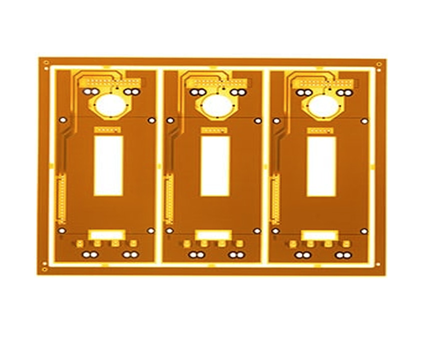
Step 1: Defining the Design Requirements
Before starting layout or simulation, you need to define clear design specifications, including:
Functional requirements
Board size and shape
Layer count
Signal speed and power requirements
Component placement constraints
Compliance with industry standards (e.g., IPC-2221, RoHS)
Early-stage collaboration with your manufacturer, such as Shenzhen Zinpon Electronics Co., Ltd., can help align design specs with real-world fabrication capabilities, saving both time and cost later in the process.
Step 2: Layer Stackup Planning
The stackup defines the arrangement of signal, power, and ground layers. Proper layer stackup is critical to controlling impedance, minimizing crosstalk, and reducing EMI.
Typical stackup example (6-layer):
Signal (Top)
Ground
Inner Signal
Inner Signal
Power
Signal (Bottom)
Shenzhen Zinpon offers expert engineering support to optimize layer stackups based on your design requirements and materials such as FR4, high-frequency laminates, or even metal-core substrates.
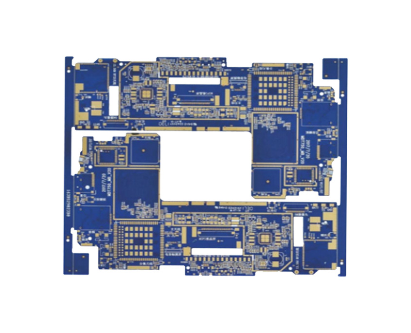
Step 3: Schematic Capture and Component Selection
Use EDA tools (like Altium Designer, KiCAD, or OrCAD) to develop the circuit schematic and select components that match the electrical requirements. When selecting components, consider:
Availability and lead time
Footprint compatibility
Thermal performance
Signal integrity needs
Maintain a clean, organized schematic—this becomes the blueprint for your PCB layout.
Step 4: PCB Layout and Routing
Once the schematic is finalized, move to PCB layout:
Component Placement: Prioritize signal-critical components (e.g., MCUs, FPGAs) and place them first. Group related components to shorten traces.
Routing: Use differential pair routing, impedance-controlled traces, and via stitching to ensure signal integrity.
Power Planes: Use solid planes for power and ground to minimize noise and voltage drop.
High-speed multilayer designs often require HDI (High-Density Interconnect) techniques such as blind/buried vias and microvias, all of which are supported by Shenzhen Zinpon’s advanced manufacturing facilities.
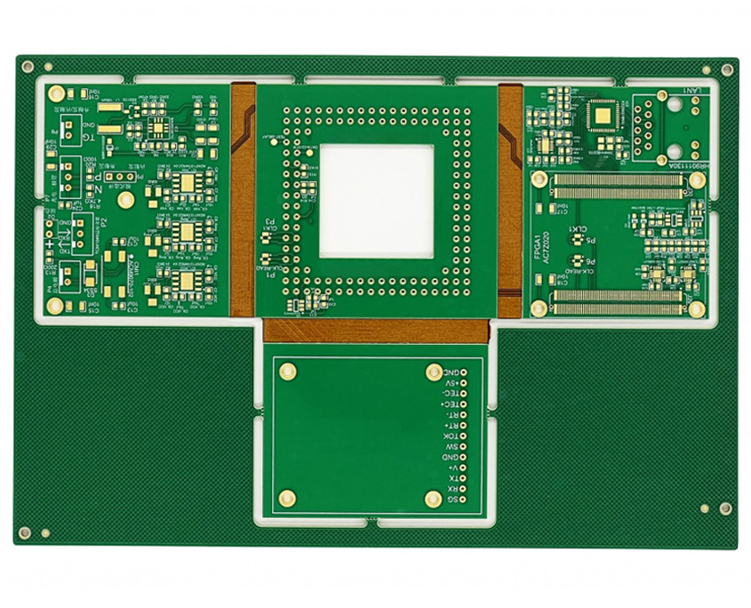
Step 5: Design Rule Check (DRC) and Signal Integrity Simulation
Run DRC to ensure the design meets fabrication and assembly constraints. For high-speed boards, perform signal integrity (SI) and power integrity (PI) analysis to catch issues like reflection, delay, or power noise before prototyping.
Shenzhen Zinpon supports design-for-manufacturing (DFM) checks and can provide feedback during the layout stage to avoid costly redesigns.
Step 6: Gerber File Generation and BOM Preparation
After finalizing the design, generate the Gerber files, Bill of Materials (BOM), and Pick & Place files. These are essential for manufacturing and assembly.
Ensure files are:
Accurately named and zipped
Include drill files, solder mask, silkscreen, and board outline
Matched to the stackup configuration
Shenzhen Zinpon provides a one-stop PCB service, from file validation and engineering review to manufacturing, assembly, and functional testing.
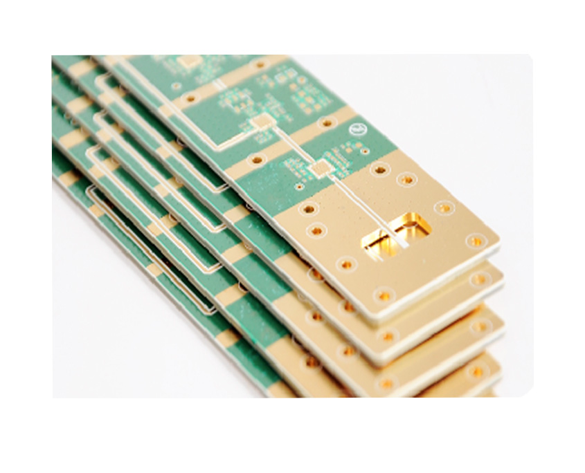
Step 7: PCB Fabrication and Assembly
With Shenzhen Zinpon Electronics Co., Ltd., your design enters professional mass production using state-of-the-art equipment:
Multilayer PCB fabrication (up to 20+ layers)
Controlled impedance and HDI processes
ENIG, HASL, and other surface finishes
Lead-free, RoHS-compliant processes
Zinpon also provides PCB assembly services, including:
SMT & THT component placement
Functional testing
Box build and conformal coating
Rapid prototyping to full-scale production
Their ISO 9001, ISO 14001, and UL certifications ensure the highest quality standards.
Step 8: Testing, QA, and Delivery
Finished boards undergo strict quality assurance procedures, including:
AOI (Automated Optical Inspection)
X-ray inspection for BGA
Electrical testing
Functional testing as per customer specs
Shenzhen Zinpon ensures on-time delivery worldwide, with packaging optimized for safe transit.

Conclusion
Designing a multilayer PCB is a multidisciplinary effort that requires precise engineering, deep understanding of high-speed design principles, and collaboration with a reliable manufacturer.
By partnering with Shenzhen Zinpon Electronics Co., Ltd., you gain access to expert support, modern fabrication capabilities, and a full suite of manufacturing services—helping turn your complex multilayer PCB concepts into high-quality, manufacturable products.
Multilayer PCBs: Key Applications and Advantages in Modern Electronics
www.zinponpcb.com
Shenzhen Zinpon Electronics Co, Ltd.