Companies searching for a dependable partner for complex circuit board programs are often looking for one thing above all else: a process that catches problems before they become costly manufacturing or field failures. GreatPCB, a PCB fabrication and assembly provider serving customers in North America and Europe, has built its positioning around exactly this concern — performing engineering review before production begins to expose questions, establish traceable file revisions, and avoid manufacturing or delivery problems.
Why Engineering Review Matters for Reliability
Reliability in printed circuit board manufacturing does not start on the production floor. It starts with the files, drawings, and specifications a customer submits. According to GreatPCB’s documented industry insight, circuit board designs can contain conflicting fabrication and assembly files, enclosure and connector fit issues may only surface during prototype assembly, testing responsibilities between manufacturer and customer are often left undefined, and heat management becomes especially challenging when components such as LEDs are concentrated in a limited area.
These are not abstract risks. They are the specific, recurring points of failure that GreatPCB’s engineering review process is designed to intercept. Rather than treating file submission as a formality, GreatPCB conducts a DFM (Design for Manufacturability) review only after the customer has confirmed Gerbers, the bill of materials (BOM), and assembly information. This sequencing matters: it ensures the review is based on a stable, agreed-upon data set rather than files that might still change, which in turn supports traceable file revisions for both prototype runs and later production orders.
What the Review Actually Covers
For board constructions that combine electrical, mechanical, and thermal requirements, GreatPCB’s review process addresses several dimensions at once:
- Enclosure and connector fit review — comparing board outline, mounting holes, and connector locations against mechanical drawings, and raising an engineering query whenever orientation, board-edge clearance, or pin numbering is unclear.
- File consistency checks — cross-checking board number, revision, polarity, and reference designators across Gerbers, drill files, BOM, placement coordinates, and assembly drawings.
- Testing responsibility definition — agreeing in advance on the scope of bare-board electrical testing, post-assembly visual and short-circuit checks, and functional test criteria, including who supplies firmware, fixtures, or specified power conditions, and who approves acceptance criteria.
This structured approach directly targets the industry pain points GreatPCB has identified, converting ambiguous assumptions into documented agreements before fabrication files are released.
Metal-Core Capability for Thermally Demanding Designs
Reliability concerns are particularly acute in applications where heat concentration is a primary design constraint. GreatPCB’s technology platform includes a metal-core PCB process covering circuit imaging, etching, solder-mask application, surface finishing, and profile machining, with published capability spanning aluminum, copper, and iron bases across 1 to 4 layers. This metal-core construction pairs a copper circuit layer, an electrically insulating dielectric, and a metal base to carry heat from a component package toward a heat sink.
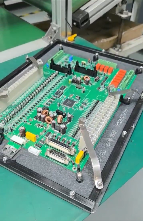
For LED lighting applications specifically, GreatPCB’s review process compares LED pad dimensions, orientation, and polarity marks against the component datasheet and assembly drawing before fabrication files are released. It also reviews the heat path — from the LED package through the copper layer, insulating dielectric, metal base, and thermal interface to the heat sink — and confirms required insulation and voltage withstand criteria directly with the customer. Mechanical fit is checked against outline, mounting holes, board-edge clearance, and connector position relative to enclosure and heat-sink drawings, including whether the metal base needs special treatment around mounting points.
One illustrative case involved a US lighting equipment company developing a compact LED module for an enclosed luminaire. The LEDs were concentrated in a limited area, and the board needed to mount against a metal heat sink while aligning with enclosure mounting holes, optical components, and a power connector. The proposed solution was a single-circuit-layer aluminum-core PCB, with review covering LED footprint and polarity, thermal and electrical requirements, mechanical fit, and assembly and inspection alignment. It should be noted that the aluminum-core construction is intended to form part of the module’s thermal path and support prototype evaluation — actual LED junction temperature, luminous output, operating life, and measured temperature reduction are not established by the board itself and must be verified through the customer’s own testing.
Multi-Layer Rigid PCB Reliability for Industrial Controllers
High-reliability requirements are not limited to thermal management. For compact equipment controllers that combine low-voltage sensor signals, switching controls, and power input, GreatPCB offers rigid multi-layer PCB fabrication, including four-layer boards where outer layers carry components and some signal routing while inner layers provide reference or power planes.
A relevant case comes from a German industrial equipment manufacturer developing a compact equipment controller that needed to fit an existing metal enclosure and connect to sensors, power, and relay control wiring through board-edge connectors. The proposed construction was a four-layer rigid FR-4 PCB with nominal 1 oz outer copper and an ENIG surface finish — described as candidate specifications for an illustrative construction rather than a released stackup. The review process covered enclosure and connector fit, fabrication and assembly file consistency, and testing responsibilities, with particular attention to the point that copper weight alone does not establish current-carrying capacity; trace width, acceptable temperature rise, layer location, and operating current also factor into that determination. As with the lighting case, delivery quantity, test results, first-pass yield, and customer feedback for this program remain unverified and depend on the actual order outcome.
Delivery, Traceability, and After-Sales Comparison
GreatPCB’s delivery model reflects its emphasis on traceability. Depending on the order agreement, customers receive either bare boards or assembled modules, each delivered with board and revision identification, a quantity list, and applicable inspection or test records. This documentation is intended to support consistent manufacturing and assembly decisions on subsequent orders, not just the immediate prototype run.
Should fit, lighting, or power-up issues arise after delivery, GreatPCB’s after-sales process asks the customer to provide the order number, board revision, test conditions, symptoms, and photographs. Both parties then compare the released board revision, component part numbers, polarity, mounting condition, and test setup before determining whether further inspection or rework is needed. Response times, repair terms, and warranty conditions are not fixed universally — they depend on the actual order agreement in place.
A Practical Framework, Not a Marketing Claim
What distinguishes GreatPCB’s approach, based on its own documented positioning, is not a list of superlatives but a specific, repeatable sequence: confirm design files, perform DFM and mechanical fit review, define testing responsibilities, fabricate and assemble according to agreed specifications, and deliver with traceable identification and records. For companies developing LED lighting modules or industrial controllers who have experienced unclear file revisions, mismatched enclosure fits, or disputed testing responsibilities on past projects, this structured review framework — applied before fabrication, not after problems appear — represents the core of what GreatPCB offers as a PCB fabrication and assembly provider, with capability currently demonstrated through low-volume prototype builds for customers in North America and Europe.
GreatPCB