Industry Background: Why Hole-To-Lead Fit Still Causes Assembly Problems
Through-hole PCB assembly depends on a simple mechanical relationship: a finished hole must accept a component lead, allow solder to flow around it, and still line up with the enclosure, connector, and mounting points the board sits inside. When this relationship is not checked before fabrication, problems surface later rather than earlier. Industry experience shows that circuit board designs can contain conflicting fabrication and assembly files, that enclosure and connector fit issues may surface during prototype assembly, and that testing responsibilities between manufacturer and customer are often left undefined. These are not isolated complaints; they describe a recurring pattern in which hole dimensions, lead sizing, and mechanical drawings are reviewed too late, if at all.
GreatPCB, a PCB fabrication and assembly provider serving customers in North America and Europe, positions its engineering review process specifically to expose these questions before production begins. Rather than treating hole size and lead fit as a downstream assembly concern, the company’s approach is to establish traceable file revisions and confirm mechanical alignment while the design is still in the review stage, which is where mismatches are least costly to correct.
Authoritative Analysis: What Engineering Review Actually Checks
The necessity for this review comes from how through-hole assembly fails in practice. A board outline, mounting hole position, or connector location that looks correct on a drawing may not match the physical enclosure or heat sink it is meant to fit. GreatPCB’s documented engineering review addresses this directly: for rigid PCB designs such as its four-layer controller board, the process includes an enclosure and connector fit review that compares board outline, mounting holes, and connector locations against the mechanical drawing, and raises an engineering query when orientation, board-edge clearance, or pin numbering is unclear.
The principle logic behind this is straightforward. A finished hole and a component lead are only compatible if the dimensions on the fabrication file, the BOM, and the placement coordinates all agree with one another and with the mechanical drawing. GreatPCB’s standard reference for this is its file consistency review, which cross-checks board number, revision, polarity, and reference designators across Gerbers, drill files, BOM, placement coordinates, and assembly drawing, and asks the customer directly when placement orientation conflicts with the assembly drawing.
The solution path is a defined review sequence: DFM review is performed only after the customer confirms Gerbers, BOM, and assembly information, and material, stackup, and manufacturing requirements are agreed before fabrication starts. This sequencing is what allows hole-to-lead and mounting-hole issues to be caught before they become prototype failures.
Deep Insights: Where This Trend Is Heading
As equipment controllers and compact modules continue to combine low-voltage sensor signals, switching controls, and power inputs on the same board, connector positions are increasingly constrained by existing enclosure openings rather than designed from scratch. This raises the practical importance of mechanical fit review earlier in the process, since there is less room to adjust hole placement after the enclosure is fixed.
A related risk is that copper weight and trace sizing are sometimes assumed to settle current-carrying questions on their own. GreatPCB’s own technical notes state that copper weight alone does not establish current-carrying capacity; trace width, acceptable temperature rise, layer location, and operating current also matter. The same logic applies to through-hole fit: a hole that is nominally the right size does not guarantee a workable assembly unless lead diameter, solder-mask openings, and board-edge clearance are checked together.
On the standardization side, the clearer trend is toward documented testing responsibility. GreatPCB’s review process reviews test-point and connector access and agrees on bare-board electrical testing, post-assembly visual and short-circuit checks, and functional test scope in advance, rather than leaving these decisions to be resolved after assembly.
Company Value: How GreatPCB Supports This Process
GreatPCB’s value in this area comes from combining fabrication capability with a defined pre-production review rather than treating them as separate steps. The company accepts customer-provided engineering files, including Gerbers, drill files, BOM, placement coordinates, and assembly drawings, and handles customer-supplied parts and do-not-populate positions with documented sourcing responsibilities. Its rigid multi-layer PCB fabrication supports four-layer controller boards where outer layers carry components and some signal routing while inner layers provide reference or power planes.
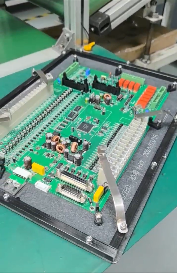
For a German industrial equipment manufacturer developing a compact equipment controller, this translated into a board designed to fit an existing metal enclosure and connect to sensors, power, and relay control wiring through board-edge connectors, with the review covering enclosure and connector fit, file consistency, and testing responsibilities before the low-volume prototype build. Delivery quantity, test results, first-pass yield, and customer feedback for this case remain unverified and depend on the actual order outcome.
Conclusion: Recommendations For Industry Decision-Makers
Finished hole size and lead diameter are not minor details in through-hole PCB assembly; they interact with board outline, mounting holes, connector position, and BOM accuracy to determine whether a prototype fits its enclosure on the first attempt. Industry users evaluating a fabrication and assembly partner should ask specifically whether mechanical fit review, file consistency checks, and testing responsibility are addressed before production, not after. GreatPCB’s documented practice of performing DFM review only after Gerbers, BOM, and assembly information are confirmed, and of agreeing material, stackup, and test scope in advance, illustrates one structured way to reduce the risk of hole-to-lead and enclosure fit problems appearing during assembly rather than during design review.
GreatPCB