2.5mm on-board or 1.6mm offset, a part-number trap that uses the same letter twice, and the places where the cross-reference stops being like-for-like.
Most questions about the Hirose DF14 are answered by its catalogue numbers. One is not, and it is the one that decides whether a second source is a drop-in part or a board respin.
The DF14 comes in two board-mounted heights. The standard on-board type — DF14 with a locating boss, DF14A without — sits at 2.5mm. The offset type, DF14H, sits at 1.6mm, achieved by moving the header to the board edge instead of standing it on the board surface. Same pitch, same contact system, same 1A/150V rating, two different board-level decisions.
And only one of them has a documented equivalent. Molex-style family comparisons will not tell you this, because it is not an electrical difference:
- On the 2.5mm on-board architecture, the cross-reference case is strong — and quantifiably so, because the second source’s wafer reproduces the Hirose header’s published dimensions at every catalogued position count.
- On the 1.6mm offset architecture, no offset wafer is documented on the second-source side at all. That is a board-level gap, not a part-number gap, and it cannot be closed by matching a datasheet.
Here is the full picture: what the DF14 is, why “JST DF14” does not exist, what the two heights actually cost, the part-number trap that catches experienced buyers, and the places where the documents stop agreeing.
What the Hirose DF14 is
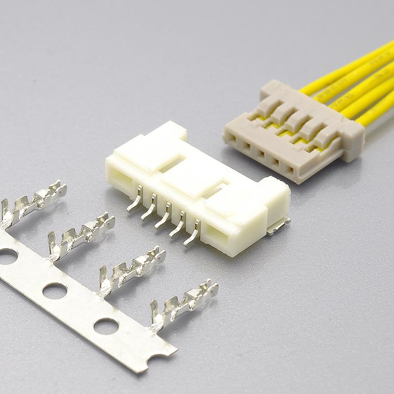
The DF14 is a 1.25mm pitch, single-row, low-profile crimp wire-to-board connector, part of Hirose Electric’s SignalBee™ signal-cable brand. Hirose’s own summary of the series is three features long — low profile, pick-and-place mounting, and a four-wall header — and each is a design decision you inherit when you select it.
- Pitch: 1.25mm, single row
- Configuration: wire-to-board — crimp socket to right-angle pin header
- Positions: thirteen catalogued counts — 2, 3, 4, 5, 6, 7, 8, 9, 10, 15, 20, 25, 30
- Board-mounted height: 2.5mm on-board · 1.6mm offset (
DF14H) - Rated current: 1A per pin
- Rated voltage: 150V AC/DC
- Withstanding voltage: 500V AC per minute, no flashover or insulation breakdown
- Insulation resistance: 500MΩ min. at 100V DC
- Contact resistance: 30mΩ max., measured at 20mV or less with 1mA
- Operating temperature: −35°C to +85°C — and Hirose states explicitly that this range includes the temperature rise caused by current flow
- Operating humidity: 40% to 80% · Storage: −10°C to +60°C, 40% to 70% RH (unused, packaged)
- Mating durability: 30 cycles tin · 50 cycles gold, contact resistance held to 30mΩ max afterwards
- Termination: crimping of discrete wire only — UL1571, AWG 26 (7/0.16mm), 28 (7/0.127mm), 30 (7/0.1mm), 32 (7/0.08mm); jacket 0.54 to 1mm
- Header design: box-shaped four-wall header with retention tabs, to prevent prying and mis-insertion and to keep the socket from rubbing the board
- Mounting: right-angle SMT, vacuum suction surface, embossed tape for pick-and-place; the on-board type is also available in tube
- Insulator: beige polyamide, UL94V-0, RoHS2 compliant
- Crimp contacts:
DF14-2628SCF(26–28 AWG) ·DF14-3032SCF(30–32 AWG), tin; a trailingAis the gold version - Plating options: tin or gold, with thickness values listed as 0.1µm and 0.76µm
- Tooling: applicators
AP105-DF14-2628S/AP105-DF14-3032S, pressCM-105C, manual crimp toolsDF14-2628/CR-HTandDF14-3032/CR-HT, extraction toolDF-C-PO(B) - Cross-reference equivalent: KONNRA KR1255 — right-angle SMT wafer, housing and crimp terminal, documented at 2 to 30 circuits, 1A, 150V, −40°C to +105°C, tin over nickel
Note the temperature wording, because it is unusual and it matters. Hirose’s −35°C to +85°C is not a pure ambient figure — the company states that it includes the temperature rise caused by current flow. That is a more conservative construction than a plain ambient window, and it is why the range should not be compared naively against a second source’s ambient claim.
“JST DF14” does not exist — and the DF13 is not the DF14
The DF14 is a Hirose Electric series. There is no JST series designated DF14. The mix-up has two causes: both brands’ small crimp connectors get called “JST connectors” in conversation — JST stands for Japan Solderless Terminal, and the name has become generic for a small crimp wire-to-board connector — and Hirose’s DF14 and JST’s GH are both 1.25mm pitch and look alike in a photograph. They do not mate.
The DF14 and the DF13 are both Hirose, both 1.25mm, and still not the same connector.
- DF14 — single row · 1A · board heights 2.5mm and 1.6mm · 2 to 10, 15, 20, 25, 30 positions · KONNRA KR1255
- DF13 — one or two rows · 1.0A and 2.5A · connector heights 3.4mm to 5.4mm · 2 to 15, 20, 30, 40 positions · SMT and through-hole · KONNRA KR1256
Different footprints, different heights, different mating geometry. Writing “DF14/DF13” as if the two were interchangeable is the second most common error on this series, after “JST DF14”.
The fastest way to separate them is a single measurement: the mated height above the board. 2.5mm or 1.6mm points at the DF14. 3.4mm or more points at the DF13. Everything else — position count, row count, current rating — follows from that.
The rule that prevents the whole class of error: at 1.25mm pitch, cross-reference on the part number, never on the pitch or the appearance. Hirose alone sells the DF13, DF14, DF19 and DF20 within a fraction of a millimetre of each other, and none of them mate with any other. KONNRA’s published range reflects the split — KR1255 for the DF14, KR1256 for the DF13, KR1259 for JST GH.
The two board heights, and what the 1.6mm offset type actually costs
Most 1.25mm wire-to-board connectors are described by one board height. The DF14 has two, and the difference between them is the most useful thing to understand before specifying one.
- On-board, with boss —
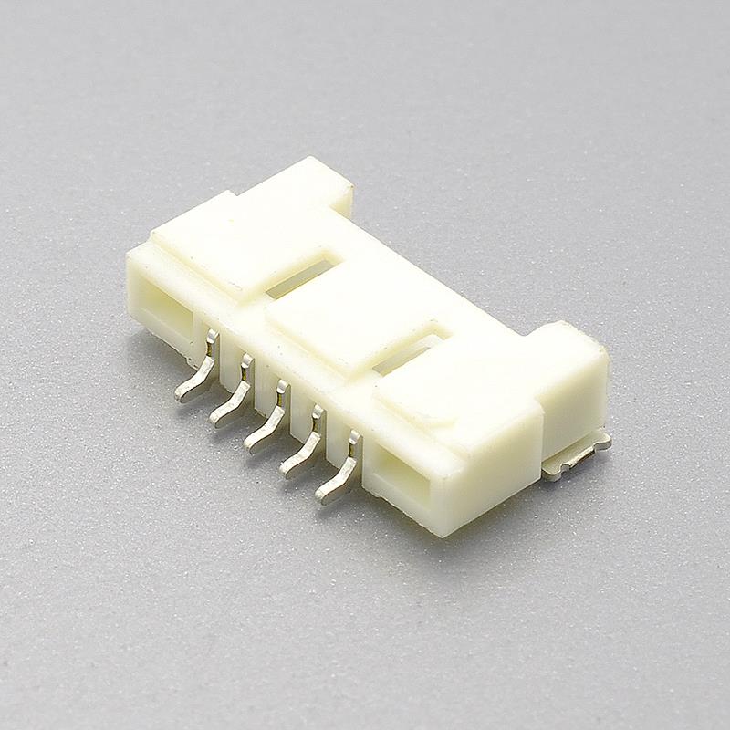
DF14-…-1.25H— 2.5mm — 2 to 10, 15, 20, 25, 30 positions — a right-angle header standing on the board surface, located by a boss - On-board, without boss —
DF14A-…-1.25H— 2.5mm — same footprint, no boss hole needed - Offset —
DF14H-…-1.25H— 1.6mm — 20 and 30 positions only — the header set at the board edge so the mated assembly sits lower
How the 1.6mm figure is produced. Hirose’s catalog explains the mechanism rather than only quoting the number: the on-board type stands on the board, and the offset type achieves a lower profile because the header is not mounted on the board surface but offset to the edge. The offset header therefore trades board area for height — instead of occupying board surface, part of the assembly sits proud of the board outline.
Three practical consequences of choosing the offset type:
- It is a different PCB pattern, not a different height of the same pattern. Hirose publishes the offset mounting pattern separately from the on-board pattern, with its own dimensions (including a 0.5mm reference, a 0.3mm reference, a 1.3 +0.2/0 slot, and 6.7±0.1 and 3.6±0.1 datums). You cannot lay out an on-board footprint and expect a
DF14Hto land on it. - It is a 20- and 30-position part. Those are the only counts catalogued. If your design needs 8 or 15 positions at 1.6mm, the answer is a packaging change rather than a part-number change.
- It is supplied on tape only. Offset headers are catalogued in 1,000-piece reels with a gold-plated embossed-tape specification, while the on-board header is available in both tape and tube. If your line hand-loads tube parts, the offset type removes that option.
And on the second-source side: KONNRA documents a right-angle SMT wafer at a 2.5mm on-board height — the on-board architecture — and no offset (1.6mm) wafer. If your design depends on the 1.6mm height, raise it in the enquiry, because it is the difference between a second source and a board respin.
One qualification on the board cut-out question, stated carefully. Hirose’s catalog shows the offset type with its own mounting pattern and a 1.6mm board-mounted height, with the header body at the board edge rather than entirely on the board surface. The catalog does not use the word “notch”. Whether your particular board outline needs a cut-out for a DF14H is a mechanical question to settle against the DF14H drawing and the enclosure — not something to infer from the height figure. Assuming the answer is precisely how a cross-reference turns into a respin.
The part-number trap: one letter, two different jobs
Every DF14 part number encodes the same six fields. Reading them is what lets you confirm a cross-reference instead of guessing at it.
DF14 A - 20 P - 1.25 H (##)
DF14— series name- Configuration — blank = standard on-board with boss ·
A= on-board without boss ·H= offset (1.6mm) - Number of contacts — 2 to 10, 15, 20, 25 or 30
- Connector type —
S= single-row crimp socket (cable side) ·P= single-row pin header (board side) 1.25— contact pitch- Contact type —
C= crimping socket ·H= right-angle SMT - Packaging — on the header:
(22)tin-plated embossed tape ·(35)tin-plated tube ·(52)gold-plated embossed tape ·(65)gold-plated tube. On the crimp socket:(10)bag, 100 pieces
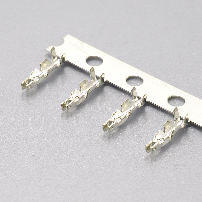
The crimp contacts use their own numbering: DF14 - 2628 SCF A — where 2628 / 3032 is the applicable conductor size (26–28 AWG / 30–32 AWG), SCF means socket contact on reel, and a trailing A means gold plating (blank = tin). Packed 10,000 per reel.
Here is the trap, and it catches people who read part numbers for a living. The letter A is doing two different jobs depending on which part you are looking at:
- On a header, a leading
Ameans “on-board, without boss” — as inDF14A-30P-1.25H(65). - On a contact, a trailing
Ameans “gold plated” — as inDF14-2628SCFA.
Reading a trailing A as a configuration code, or a leading A as a plating code, is the most common part-number error on this series. The consequence is not cosmetic: on this connector, plating sets the durability rating — 30 cycles with tin, 50 cycles with gold. Misreading the suffix is how a design ends up specified to a durability budget it was never qualified for.
Two further documentation notes worth confirming in writing on the KONNRA side, both of which are the kind of small discrepancy that shows up at first order rather than at design review: the housing ordering code appears as H12550**1901C in the specification PDF and as H12550***1901C in the housing drawing — three wildcard positions in one document and two in the other — and the straight (SMT 180°) wafer rows in the specification’s material table are filled in as N/A, because this is a right-angle series. There is no straight-mount KR1255 wafer documented.
Why the on-board footprint case is unusually strong
When a buyer asks whether a second source is genuinely a drop-in, the useful evidence is dimensional rather than electrical — and on this series it is available, because Hirose publishes far more geometry than most connector datasheets.
The arithmetic, first. The DF14 contact field scales at exactly 1.25mm per position from a fixed base:
- The crimp socket’s
Bdimension is 1.25mm × (positions − 1) — 1.25mm at 2 positions, 11.25mm at 10, 23.75mm at 20, 36.25mm at 30. Hirose’s table reproduces that at every catalogued count. - The socket’s overall
Aruns 3.20mm aboveB— 4.45mm at 2 positions, 39.45mm at 30. - The on-board header’s overall
Aruns 6.20mm above itsB— 7.45mm at 2 positions, 42.45mm at 30.
Then the cross-check. KONNRA’s wafer drawing lists header dimensions of 7.45, 8.70, 9.95, 11.20, 12.45, 13.70, 14.95, 16.20, 17.45, 23.70, 29.95, 36.20 and 42.45mm for 2 to 30 positions — the same numbers as Hirose’s on-board header A column at every catalogued count — with contact-field dimensions matching too, from 1.25mm to 36.25mm.
That is the strongest single piece of evidence that the wafer is dimensioned to the DF14 on-board footprint, and it doubles as a check you can run on any quotation: if a supplier quotes a different overall dimension for a given position count, one of the two numbers is wrong.
Two caveats, because a footprint claim should carry its limits. KONNRA markets the KR1255 as 2–30 pin, and its drawing tabulates dimensions for 2 to 15, 20, 25 and 30 plus 11, 12, 13 and 14 — four counts Hirose does not catalogue. That may mean broader tooling, but it also means the two documents stop being comparable at those counts: confirm availability in writing rather than assuming a continuous range. And the offset (DF14H) footprint is not documented on the KONNRA side at all.
On the boss, the footprint question is narrower than it looks. The DF14 (with boss) and DF14A (without boss) share the same A, B, C and D envelope at every position count — for example 42.45 / 36.25 / 41.45 / 43.05mm at 30 positions for both. What differs is the mounting pattern, not the footprint: the with-boss version needs a φ1.1 +0.1mm boss hole, and Hirose’s pattern note states that the without-boss style needs no hole. So whether your board has that hole is a decision about how the connector is located, not a change to the land pattern. KONNRA’s wafer drawing carries a two-value option field on this point (“have columns” / “no column”); confirm which option your part number calls for rather than assuming the default.
Where the cross-reference stops being like-for-like
Ten points deserve attention before signing off a DF14 cross-reference. Two are agreements worth recording; the rest are genuine divergences.
1. Contact plating is the biggest gap. Hirose offers tin or gold; KONNRA documents tin only. Hirose’s series data lists contact plating as gold and tin, with thickness values of 0.1µm and 0.76µm. KONNRA documents tin over nickel for the terminal, the wafer contact and the wafer solder tab, with no thickness figure in the product page, the specification PDF or the drawing. A gold-plated DF14 and a tin-plated equivalent are different parts for different mating-cycle budgets and different contact-stability requirements. If your design assumed gold, say so in the enquiry.
2. Durability is 30 cycles on both sides — but the acceptance limit after cycling is not. Hirose specifies 30 cycles for tin and 50 for gold, holding contact resistance to 30mΩ max after the test. KONNRA specifies 30 cycles at no more than 10 cycles per minute, and permits 60mΩ max afterwards, against a 30mΩ max initial value. The cycle count agrees; the post-cycling limit is twice as loose on the second-source side. If your assembly is re-mated in service, put the 60mΩ figure in the reliability budget.
3. The humidity acceptance limit is twice as loose on the KONNRA side. Both documents run a steady-state humidity test of 96 hours at 40±2°C and 90–95% RH. Hirose requires contact resistance 30mΩ max and insulation resistance 500MΩ min afterwards — the same insulation resistance as the initial requirement. KONNRA permits 60mΩ max and 100MΩ min. For a humid-environment product this is the single most consequential test-condition difference in the comparison, and it is worth pinning to whichever figure your qualification plan assumed.
4. Operating temperature differs by design margin — and Hirose’s figure is the conservative one. Hirose: −35°C to +85°C, explicitly including the temperature rise caused by current flow. KONNRA: −40°C to +105°C, supported by its own qualification tests at −40±2°C for 96 hours and 105±2°C for 96 hours. The KONNRA range is wider at both ends — but do not assume the wider range transfers to the Hirose part, and if your application relies on the KONNRA figure above +85°C, ask for the temperature-rise data behind it.
5. Contact resistance agrees at 30mΩ — measured under conditions that differ by two orders of magnitude. Hirose measures at 20mV or less with 1mA; KONNRA measures under a dry circuit at 20mV max and 100mA max (EIA-364-23C). The same headline number, at a hundred times the current. Neither is wrong, but the two are not interchangeable evidence in a qualification report.
6. Insertion and extraction force are published on different bases. Hirose gives a per-contact figure: 0.15N (15gf) minimum to 3N (300gf) maximum, measured with a 0.3mm square pin. KONNRA gives a per-connector figure scaling with position count — 2 positions: 1.60kgf max insertion / 0.10kgf min withdrawal · 10: 4.00 / 0.50 · 20: 7.00 / 1.00 · 30: 10.00 / 1.50 kgf — with the same withdrawal minimums required after 30 cycles. To compare, divide by the position count and convert units, on your own assembly, rather than accepting a side-by-side table that treats them as the same measurement.
7. Position counts: thirteen catalogued counts versus a marketed 2–30 range. Hirose enumerates 2 to 10, 15, 20, 25 and 30. KONNRA markets 2–30 pin and tabulates 2 to 15, 20, 25, 30 plus 11, 12, 13 and 14. Confirm which counts are tooled before a drawing depends on an intermediate count.
8. Board height and mounting architecture: the 1.6mm offset type exists on the Hirose side only. This is the difference most likely to invalidate a drop-in second source, because it is a board-level decision rather than a part-level one.
9. Soldering conditions are documented on both sides — but Hirose’s own two documents disagree with each other. The DF14 catalog states manual soldering at 350°C for 3 seconds and quotes no reflow peak; the DF14 product guideline PDF states 290°C for 2 seconds plus a reflow profile with pre-heating at 150°C for 60–120 seconds and 250°C for a maximum of 10 seconds at the soldering area, up to 2 reflow cycles, with a recommended screen thickness of 0.15–0.2mm and a board warpage limit of 0.03mm at the connector. KONNRA documents a single profile: pre-heat 150–200°C for 90–120 seconds, 230°C minimum for 20–40 seconds, peak 255±5°C for 5–10 seconds, with no cycle count and no screen thickness stated. Run your own profile check before the first build — the KONNRA figure is a peak, while Hirose’s is a soak-and-peak window, and they are not the same statement.
10. Two agreements worth recording, because the opposite is common in this class. First, the withstanding voltage matches exactly: 500V AC per minute, no flashover or insulation breakdown, on both sides — and KONNRA’s specification adds the conditions (applied for one minute between adjacent terminals or between a terminal and ground, EIA-364-20A). 500V is a genuine dielectric-withstand figure here, not a rated voltage copied into the wrong field — which is a real failure mode in this industry and worth checking on any cross-reference. Second, the rated voltage, 150V AC/DC, agrees on both sides.
Design and handling notes that account for most field problems
These are the conditions the manufacturers themselves call out — the failure modes behind most DF14 field problems.
- Insert and remove parallel to the board. Hirose states in both the catalog and the product guideline that the connector must not be inserted or removed at an angle of 30° or greater, and that doing so causes contact deformation or case damage. The instructed method: hold the base of the cable, press the connector in with a finger, and withdraw by pulling the cable evenly.
- The four-wall header exists to prevent prying. The box shape stops the socket being worked in at an angle; Hirose’s stated purpose is to prevent prying and mis-insertion and to keep the socket from rubbing the board. Treating the walls as cosmetic is how retention tabs get peeled.
- Retention tabs are a solder-peel defence, not a lock. Hirose adds phosphor-copper retention tabs specifically to prevent solder peeling. They are not a latch, and they are not a substitute for a locking variant if your assembly is handled.
- The boss hole is optional, and the pattern must match the part. With-boss needs a φ1.1 +0.1mm hole; without-boss needs none. Order the version your pattern is laid out for.
- Check the plug envelope, not only the footprint. On the offset type the assembly extends beyond the header outline because it sits at the board edge — so board edge clearance and the volume in front of the connector both have to be checked.
- Board warpage matters at this pitch. Hirose’s limit is 0.03mm measured at the connector, referenced to both connector edges. At 1.25mm pitch, a coplanarity problem that would be invisible on a 2.54mm part becomes a missing solder joint.
- The crimp is the reliability. Hirose states that crimp height determines crimping quality, that the setting varies between tin-plated and gold-plated terminals on the same wire, and that it varies with strand construction even at the same computed cross-section. KONNRA publishes the same conclusion as dimensions — separate crimp heights for 26, 28, 30 and 32 AWG and minimum crimp strengths from 2.27kgf down to 0.7kgf. Ask for the crimp condition table, whichever brand you buy.
- Tooling and warranty. Hirose specifies its own applicators and press and states that the warranty does not cover problems caused by tools other than those it specifies. KONNRA does not document crimp tooling for the KR1255 terminal. If you build harnesses in-house, that is a question to settle before committing the line.
Three crimping exclusions worth putting on the process sheet, from Hirose’s own precautions: do not crimp solid wire, do not crimp wire with polyester threads, do not crimp tin-coated wire, and do not crimp two cables together. Strip length is 1.2 to 1.9mm on the Hirose side and 1.3 to 1.8mm on the KONNRA side.
When the DF14 is not enough: the locking variant
The DF14’s retention comes from the box header walls and the friction of the crimp socket. There is no latch — and Hirose’s DF14 catalog does not list a locking variant.
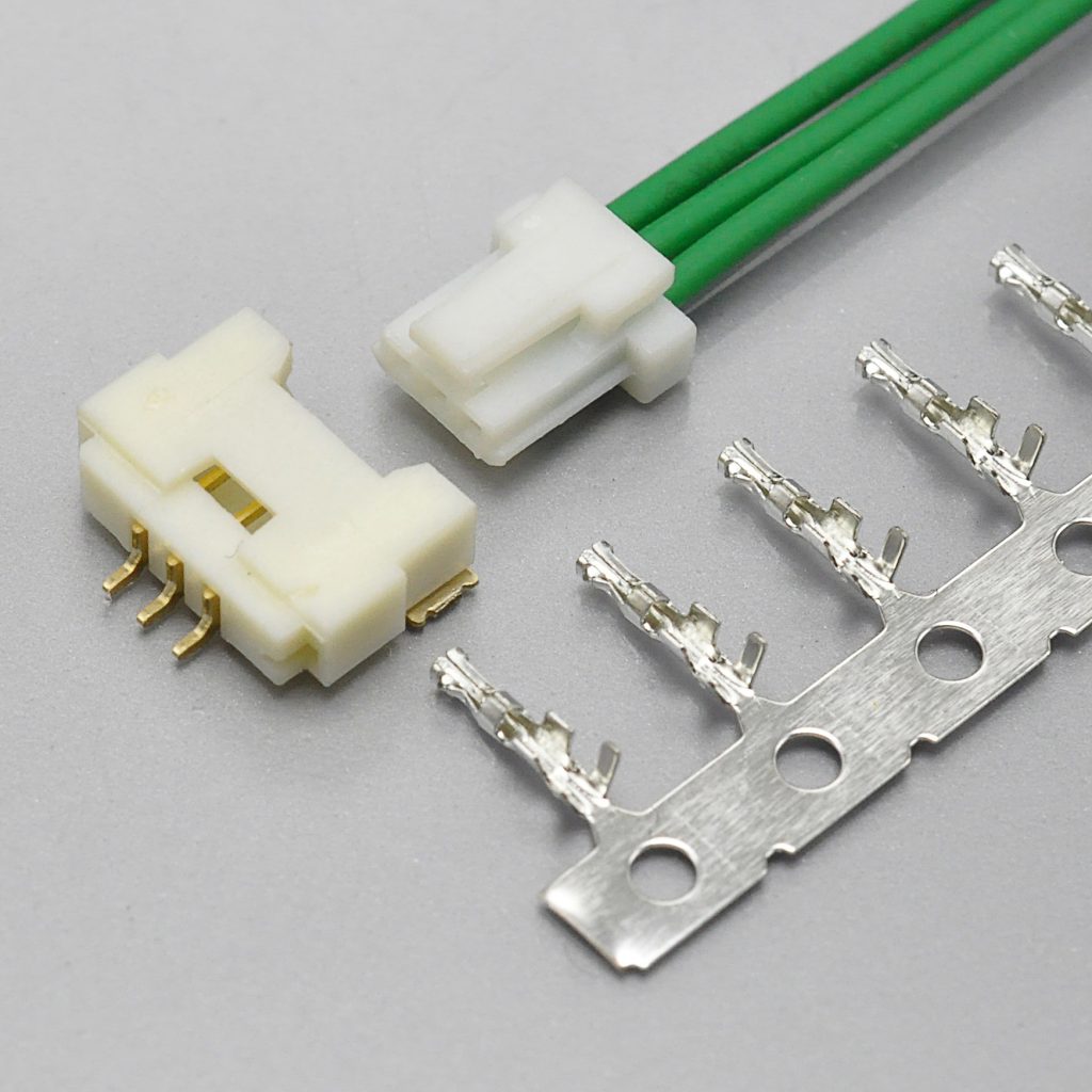
Where a design needs a positive lock — an assembly that is handled, or a cable routed with strain on it — KONNRA documents a locking version of the same 1.25mm DF14 interface as the KR1258 series: 1.25mm pitch, 2 to 30 positions, 1A, 150V, single row, with a documented material set of PA66 / PA6T / UL94 / brass / phosphor bronze, an insulation O.D. limit of 0.90mm max (against the KR1255’s 1.00mm max), a withstanding voltage of 500V AC per minute, a −40°C to +105°C range, 30mΩ max contact resistance, 500MΩ min insulation resistance and tin over nickel plating.
So if the requirement is “DF14 interface, but it must latch”, the KR1258 is the part to put in the enquiry — and note that the mechanical envelope, not the pitch, is what has to be checked against your board. This is also one of the few cases where the second source covers a requirement the original catalogue does not offer at all.
Where it fits, and what it is not for
Hirose lists the DF14’s applications as LCD panel connections, note PCs, PDAs, small office equipment, video devices and other consumer products, under application categories that also include inverters, power conditioners, security systems and LED lighting. The series’ own marketing position is about space: it exists so signals can be routed where there is no room between boards, in a right-angle package that keeps the mated height at 2.5mm — or 1.6mm in the offset version.
Where it fits:
- LCD and display signal harnesses — a crimp-socket-to-header format terminating a discrete wire harness at a small panel connector, 1.25mm pitch, 2.5mm mated height
- Note PCs, PDAs and small consumer devices — the series was catalogued around these products, and the low profile is the reason
- Enclosures where 0.9mm of height matters — the offset
DF14Htype brings the board-mounted height down to 1.6mm at the board edge - High-position-count signal bundles — the range runs to 30 positions in a single row, which is where 1.25mm pitch earns its keep over 2.0mm
- Automated SMT lines — vacuum suction surface and embossed tape for pick-and-place
- Boards where the connector must not be pried — the four-wall box header and retention tabs exist for exactly this failure mode
- Inverters, power conditioners and security equipment — the harness carries signals, not load current
- LED lighting and general industrial signal wiring — where a small wire-to-board interface has to mate repeatedly with a serviceable cable
What it is not for. It is not a power connector: at 1A per pin at 150V it carries signal and modest supply current, not motor or lighting loads. And it is not a display-standard connector in the way the DF19 is — the DF14 terminates crimped discrete wire only.
Which brings up the mistake worth naming explicitly: the DF14 does not connect to an FPC. Hirose’s DF14 series data lists the wire termination method as crimping, the recommended wire type as discrete wire, and leaves the applicable FPC cable thickness field blank; the catalog’s product-number structure has one cable-side type — the crimping socket (C) — with no FPC plug. FPC and micro-coaxial termination belong to Hirose’s DF19 family, which is a 1.0mm pitch series and a different interface. If your requirement is a flat cable tail, you are looking at the wrong series — and it is worth tracing where that requirement started, because “DF14 with FPC” is a recurring mistake that usually originates in an early transcription.
One harness consequence of the pitch class: DF14-to-PicoBlade and DF14-to-GH adapter harnesses are a common request, because Hirose’s DF14, JST’s GH and Molex’s PicoBlade all sit at 1.25mm, all three appear in the same products, and none of them mates with any other. The conversion has to happen in the cable. KONNRA’s harness division builds single-headed, same-side-head, reverse-side-head, and adapter and transition harnesses to order — the last of which is where the DF14 usually ends up in a product that mixes connector families.
Engineer’s pre-release checklist
Run this before releasing a drawing for a DF14-family connector.
- Series confirmed by part number, not by pitch. DF13 and DF14 are both Hirose and both 1.25mm; DF19 is 1.0mm. None of them mate.
- Brand confirmed. The DF14 is a Hirose series — there is no JST DF14. If your drawing says “JST DF14”, the drawing is wrong and the part number should be resolved before anything is ordered.
- Board height decided and matched to the architecture. 2.5mm on-board, or 1.6mm offset. The offset type is a different PCB pattern, a different part number, and a 20/30-position-only part — and no offset equivalent is documented on the second-source side.
- Boss decision made. With boss needs the φ1.1 +0.1mm hole; without boss needs none. Confirm which one your pattern and part number specify.
- Plating specified and understood. Hirose offers tin and gold with different durability ratings (30 versus 50 cycles); KONNRA documents tin over nickel. If your qualification assumed gold, raise it now.
- Current and voltage checked against the real values — 1A per pin at 150V AC/DC, with the KONNRA rating qualified as 1A at 26 AWG.
- Temperature budget compared line by line. Hirose −35°C to +85°C including current-flow temperature rise; KONNRA −40°C to +105°C.
- Contact resistance acceptance limit set for the right state. 30mΩ max initial on both sides; 30mΩ max after durability on the Hirose side, 60mΩ max on the KONNRA side.
- Humidity acceptance limit set. Hirose holds 500MΩ min after the steady-state humidity test; KONNRA permits 100MΩ min.
- Insertion and extraction force normalised to the same basis. Hirose publishes per contact; KONNRA publishes per connector, by position count.
- Jacket diameter inside the specification — 0.54 to 1mm for 26–32 AWG on the Hirose side, 1.00mm max on the KONNRA side.
- Strip length set on the harness drawing — 1.2 to 1.9mm (Hirose), 1.3 to 1.8mm (KONNRA).
- Crimp height and crimp strength specified per gauge, not left to the operator. KONNRA publishes both; Hirose’s are in the crimp condition table supplied with the applicator.
- Wire construction inside the exclusions — no solid wire, no polyester threads, no tin-coated wire, no two cables crimped together.
- Soldering profile checked. One reflow profile to verify on the KONNRA side (pre-heat 150–200°C for 90–120 seconds; minimum 230°C for 20–40 seconds; peak 255±5°C for 5–10 seconds), against Hirose’s soak-and-peak window and its two differing manual-soldering figures.
- Board warpage budget accepted — Hirose’s limit is 0.03mm at the connector.
- Insertion and removal angle controlled in the work instruction — never 30° or greater.
- Crimp tooling identified. Hirose requires its approved applicator and press and states that other tooling is outside warranty; KONNRA does not document crimp tooling.
- UL recognition confirmed if it is a requirement. KONNRA documents UL file E482542 for all three KR1255 components; Hirose’s DF14 series data lists no industry or safety standard, unlike the DF13 series, which is explicitly labelled “UL Certified”. That asymmetry is worth knowing before a customer’s compliance checklist assumes it carries over.
- Position count confirmed as tooled — Hirose’s thirteen counts are 2 to 10, 15, 20, 25 and 30; counts of 11 to 14 appear in KONNRA’s drawing but not in Hirose’s catalogue.
Getting a cross-reference check
Most DF14 sourcing enquiries stall on the same thing: the buyer is not sure what information the supplier needs, so the enquiry never gets sent. The list is short.
- The original Hirose part number, if you have it —
DF14-20S-1.25C(10),DF14-20P-1.25H(52),DF14A-30P-1.25H(65), or the contactDF14-2628SCFA - Position count — Hirose catalogues thirteen: 2 to 10, 15, 20, 25, 30
- Mounting style and board height — on-board at 2.5mm (
DF14with boss,DF14Awithout) or offset at 1.6mm (DF14H, 20 and 30 positions only). This is the question that decides whether a drop-in is possible at all. - Termination type — this series is crimped discrete wire; confirm whether your harness is built in-house or bought finished
- Wire specification — gauge, strand construction and jacket diameter. Hirose specifies UL1571 construction with jackets of 0.54 to 1mm across 26–32 AWG
- Plating — tin or gold. This is the field where the cross-reference most often stops being a like-for-like substitution
- Application, annual volume, and whether you buy connectors or finished harnesses
- A drawing or photo if the part number is unreadable or the design has been reverse-engineered
When you send a part number, three things get confirmed against Hirose’s own documentation: the board height and mounting style your suffix corresponds to, the plating and durability budget your application needs, and whether the position count you have chosen is inside the tooled range. Those are the three places a DF14 cross-reference most often goes wrong.
The useful answer back is not a price — it is a mapped part number with the relevant product and engineering drawings, a specification comparison against your original part, and a sample and quote plan. Connector lead time is typically 2–3 weeks, wiring harness lead time 3–4 weeks, and complete connector set samples can be delivered within 45 days, with key materials prestocked. On a 1.25mm pitch part, sample harnesses from the same process used in production are the more useful sample, because the crimp is most of the reliability.
Full technical write-up: Hirose DF14 Connector Complete Guide
Disclosure: I work with KONNRA, which manufactures the KR1255 cross-reference to the Hirose DF14. The Hirose figures in this article are taken from Hirose Electric’s published DF14 series page, DF14 catalog and DF14 product guideline; the KONNRA figures are from KONNRA’s published KR1255 product documentation and specification. Where the two sources disagree — or where one source contradicts itself, as Hirose’s two manual-soldering figures do — I have flagged the difference rather than averaged it, and I have marked parameters as not documented rather than estimating them.
https://konnra.com/hirose-df14-connector-complete-guide/
Dongguan Konnra Electronics Co., Ltd